Last time we took a look at the Terasic DE10-Nano Cyclone V SoC development board from a high-level. In this post, we’re going to be looking at setting up the DE10-Nano and getting started with the example environment and applications provided by Terasic and Intel.
The DE10-Nano kit includes:
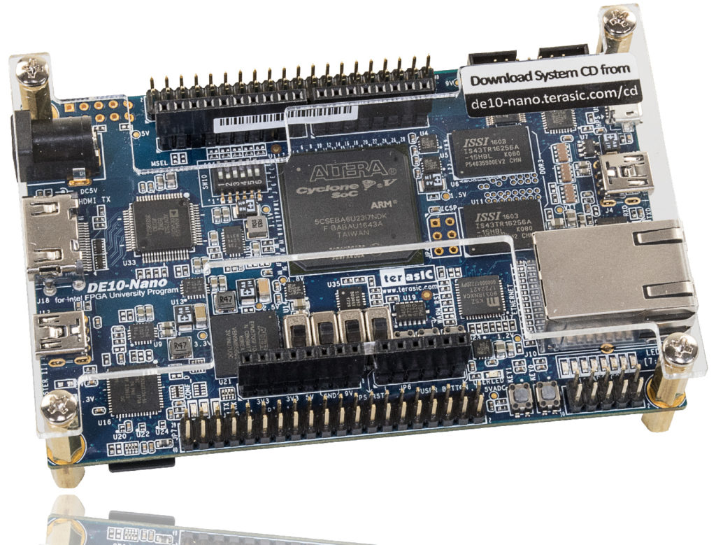
1. DE10-Nano Board, acrylic cover, and standoffs
2. DE10-Nano Quick Start Guide
3. 1x USB Type A to USB Mini-B cable
4. 1x USB Type A to USB Micro-B cable
5. 5V DC Power Adapter
6. microSD Card with example design and software (pre-installed in the microSD slot)
7. 4x Silicon foot stands (to slide over the bottom standoffs)
The USB/Mini-B cable is included for the integrated USB Blaster II JTAG programmer, while the USB/Micro-B cable can be used for either the UART to USB serial port, or for the USB On-the-Go (OTG) port. Ideally, the DE10-Nano would have included two USB/Micro-B cables to allow for simultaneous use of the USB/UART and USB OTG ports, but since it doesn’t, keep in mind that you’ll need to bring your own cable if you need that capability.
Setting up the board is very straight forward:
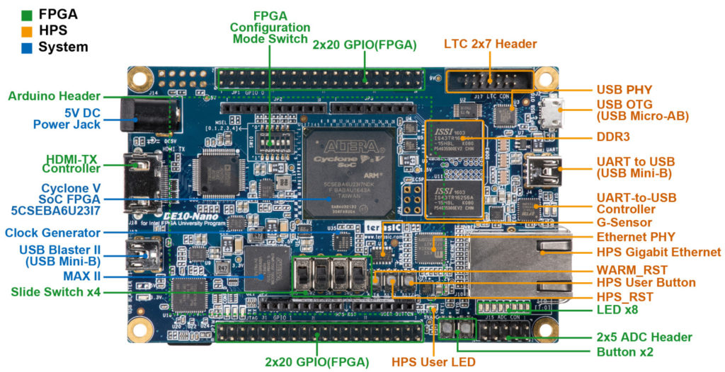
1. Ensure that the DIP switches that set the FPGA configuration mode are properly configured
2. Ensure that the microSD card is properly installed
3. Connect the USB Micro-B cable to the USB OTG port
4. Connect the power adapter to the board and an AC outlet
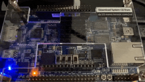
A power good LED will illuminate immediately after applying power, and after approximately 10 seconds the User LED at the front right of the board will begin blinking, indicating that Linux has booted on the SoC.
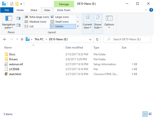
Once Linux has booted, the board should show up on your computer as a USB Mass Storage device – that is, the same way a flash drive does. On the Windows PC that I’m using with this board, it’s mapped as the E: drive. On the drive is a START.HTML file that you can open with your web browser of choice; this file includes additional instructions for getting started.
In addition to the USB Mass Storage device, the board also presents a USB RNDIS device to your computer – that is, a USB Network Adapter. For Mac and Linux users the appropriate driver will be used automatically.
Windows users aren’t so lucky. While RNDIS is a Microsoft protocol, and Windows does include appropriate RNDIS compatible drivers (as of Windows 10), the Linux environment on the DE10-Nano isn’t set up in such a way that Windows can automatically detect the correct driver. The START.HTML file on the USB Mass Storage device includes instructions on installing the included RNDIS driver; unfortunately, the instructions don’t work for users of Windows 10. Attempting to install the provided driver results in this error message:
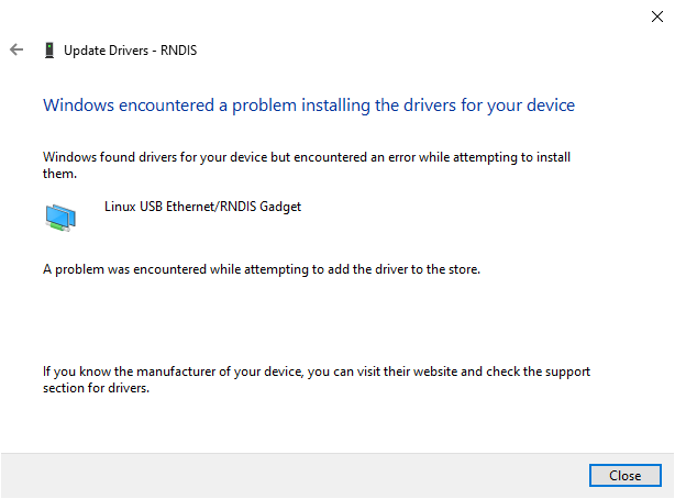
The issue (which is not well described in the error) is that Windows 10 requires the use of cryptographically signed drivers, and the driver included by Terasic is not signed. Driver signing is a security feature designed to protect users from malicious drivers; drivers run with significant privileges inside the system, and malicious drivers can cause serious problems for affected users. Driver signing attempts to mitigate this threat by requiring kernel mode drivers to be submitted to Microsoft’s “Windows Hardware Developer Center Dashboard” and be properly signed by the manufacturer.
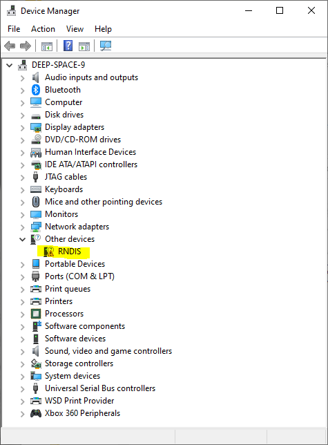
Fortunately, Windows 10 does include an appropriate driver, it just won’t automatically install it due to the configuration of the USB gadget presented by the DE10-Nano’s Linux environment. To install the compatible driver:
1. Open the Device Manager and find the RNDIS device under the “Other Device” heading
2. Right click on the RNDIS device and select “Update Driver”
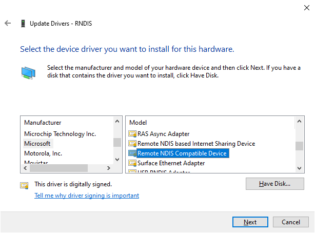
3. On the following screens, select the “Browse my computer for drivers”, “Let me pick from a list of available drivers on my computer”, and “Network adapters” options
4. Select “Microsoft” from the list of manufacturers, and “Remote NDIS Compatible Device” from the list of devices as shown below
5. Finalize the driver installation
Once installed, the “Remote NDIS Compatible Device” will appear in the “Network adapters” section of the device manager.
The DE10-Nano includes a DHCP server, so your computer will automatically obtain an IP address on the USB/RNDIS network adapter. The DHCP server is set up to provide an address on the 192.168.7.0/24 subnet, which could interfere with your local network/WiFi if your router is also configured to use this subnet (unlikely, but possible).
Once the USB/RNDIS device is set up, the DE10-Nano’s start page can be opened by navigating to 192.168.7.1 in your web browser, as shown below.
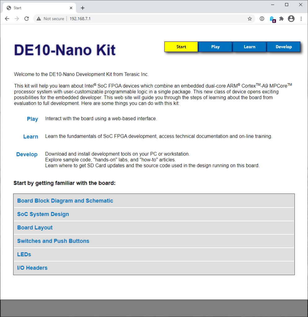
The start page consists of four primary sections:
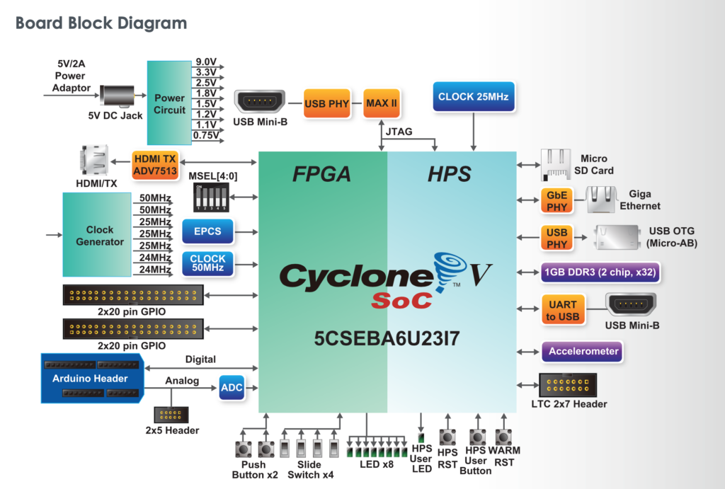
1. Start – Basic information about the board, including block diagrams, board layout, and positions of the switches, buttons, LEDs, and headers.
2. Play – Interactive demonstrations using the board’s sample designs. The first demo is “Blink the LEDs”, which allows the web application to blink on board LEDs which are connected to the FPGA fabric. The second demo is a Fast Fourier Transform (FFT) demo, which performs an FFT on a sample signal using both the ARM processor and an FFT engine in the FPGA fabric, and shows the performance difference between the two.
3. Learn – More detailed information on developing with the board and Intel SoC FPGAs, including fundamental concepts such as the boot and FPGA configuration flow, developing software and FPGA logic, and accessing FPGA peripherals from software running on the ARM processors. There are also links to Intel’s documentation and other resources.
4. Develop – Links to Intel’s development tools for both software and FPGA development, example designs and labs, and the design files used to create the included example designs.
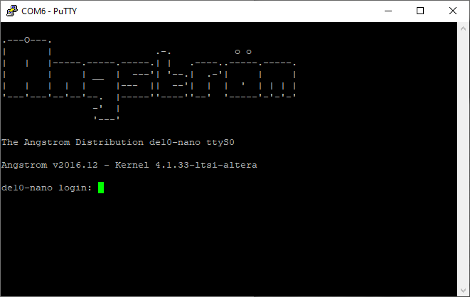
In addition to the USB/Mass Storage and USB/RNDIS devices presented over the USB OTG port, the DE10-Nano also has a USB/UART (serial port) connected to the Hard Processor System (HPS). Connecting a USB cable to this port allows you to connect to the ARM processor’s serial console, and in this case access the u-boot bootloader, Linux boot output, and a Linux command line environment. The default serial parameters are 115200, 8-N-1, and the default username is “root” with a blank password.
Finally, the default Linux distribution includes a GUI environment using the XFCE desktop environment. To use it, attach a monitor to the HDMI port, a USB-Micro A male to USB A female (OTG) adapter, a powered USB hub, and a USB keyboard and mouse.
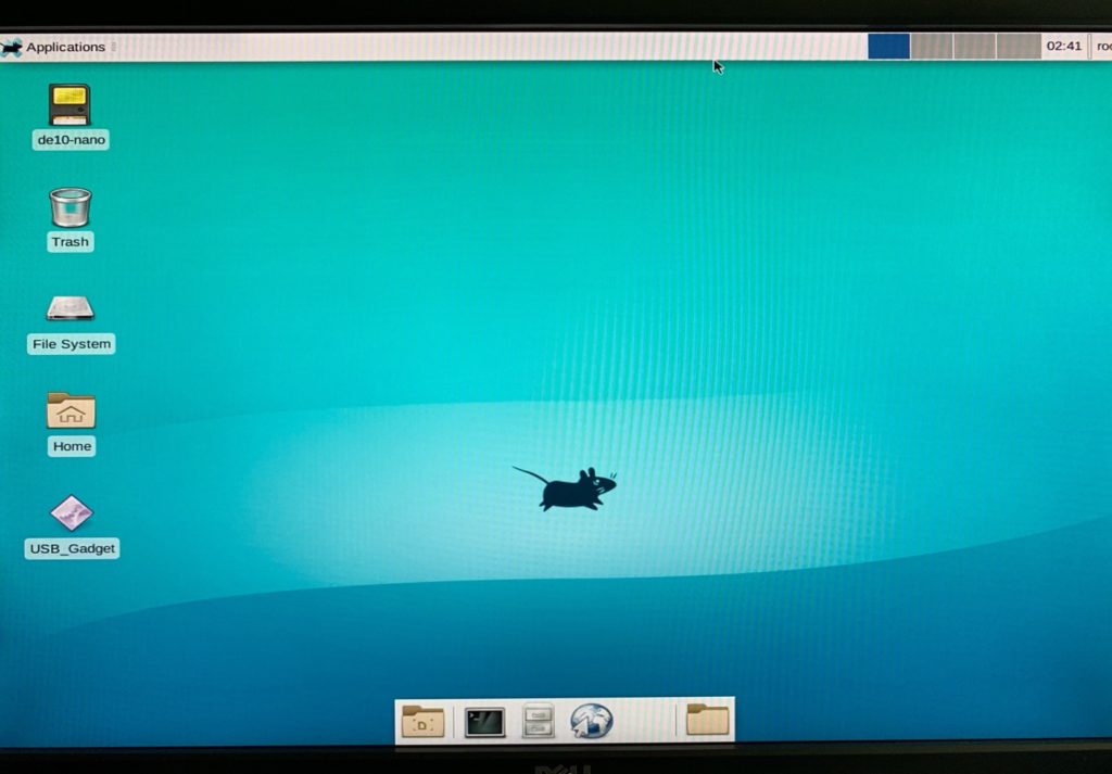
It seems perfectly serviceable, though I did experience some keyboard and mouse lag. Frankly, I wouldn’t recommend using the DE10-Nano for this purpose unless you’re using the FPGA fabric to provide some sort of acceleration, as a $35 RaspberryPi 4 is faster and more capable.
That concludes the quick start guide for the DE10-Nano. Next time we’ll look at setting up MiSTer on it, and playing with some old software.