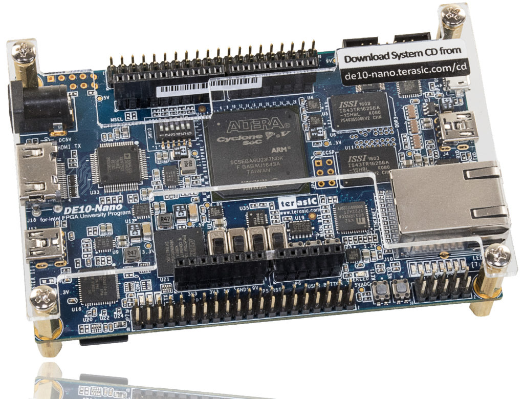
Image source: DE10-Nano Product Page
One of the items on my Christmas list this year was the Terasic DE10-Nano Cyclone V system-on-chip (SoC) FPGA development board, which forms the base platform for the MiSTer emulation/replication project. From the MiSTer wiki:
MiSTer is an open project that aims to recreate various classic computers, game consoles and arcade machines, using modern hardware.
As someone with a love of retro computing/gaming (especially classic Macs) AND FPGAs, this project is almost perfectly targeted at me, and I’m looking forward to playing with it (and hopefully contributing to it) in the future. More on that at a later date.
Since I was mostly interested in the DE10-Nano as a host for MiSTer cores, I hadn’t done much research about it in advance. Once I had it, I decided it would be worth spending some time with it as an FPGA board before diving into the MiSTer world.
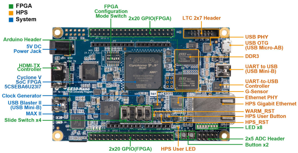
Image source: DE10-Nano Layout Page
At the heart of the DE10-Nano is one of the SoC variants of the Cyclone V, the Cyclone V SE, specifically the 5CSEBA6U23I7NDK. According to Intel’s Device Overview (PDF), this decodes as:
- 5C : Cyclone V
- SE : SoC with enhanced logic/memory
- B : No hard PCIe or hard memory controller
- A6 : 110k logic elements
- U : Ultra FineLine BGA (UBGA),
- 23 : UBGA Package type 23, 672 pins, 23x23mm
- I : Industrial temperature grade, Tj = -40C to 100C
- 7 : Speed grade 7 (middle, 6 = fastest, 8 = slowest)
- N : Lead-free packaging
- DK : ???, best guess is “Developer Kit”, to ensure that devices sold for evaluation boards aren’t resold into other channels. It could also be a customer specific part number suffix for Terasic.
As an SoC FPGA, the Cyclone V SE can be thought of as two couples, semi-independent devices: the FPGA fabric subsystem, and the ARM SoC subsystem (Hard Processor System or HPS in Intel terminology).
The FPGA fabric is the standard Cyclone V FPGA fabric, which is primarily comprised of logic blocks (Adaptive Logic Modules or ALMs), RAM blocks, and DSP (multiplier/accumulator) blocks. The HPS is comprised of a single or dual core ARM Cortex A9 processor complex, along with a DDR2/LPDDR2/DDR3 SDRAM controller, various interface peripherals (Ethernet, USB 2.0, SD/eMMC), and more – basically all of the components you’d expect to find in a comparable standalone ARM SoC. As an SoC FPGA, the FPGA fabric and processor subsystem are designed to be used in conjunction, though nothing requires you to do so.
In a future post I’ll go into more detail on reading FPGA datasheets and product guides, but for now suffice it to say this is a VERY powerful FPGA for most hobbyist (and many commercial) applications. Much larger and faster FPGAs are available on the market, including SoC variants with faster processors and more peripherals, but this is a very competent device, especially since the DE10-Nano lists for $135 USD (direct from Terasic, less with an academic discount), or $140 USD on Amazon.
In addition to the Cyclone V, the DE10-Nano has a full compliment of peripherals connected to the various interfaces provided by the Cyclone V. 1GB of DDR3 SDRAM is available for the HPS, providing ample RAM for many embedded Linux solutions and applications. USB 2.0 On-the-Go (OTG), 10/100/1000 Copper Ethernet, Micro SD, and HDMI Output are all provided. The board also integrates a built-in ByteBlaster II JTAG interface for use with the Quartus software, and a built-in USB/UART for serial console access.
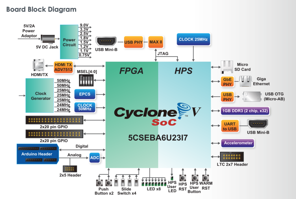
Image source: DE10-Nano Product Brief (PDF)
Some of the peripherals are directly connected to the FPGA fabric, while others are connected to the HPS. The block diagram above shows how the peripherals are allocated. Peripherals in one domain can be accessed from the other domain via the memory mapped interconnect between the two domains. For example, the ARM A9 processors running Linux can display video via the HDMI output by interfacing with HDMI pipeline logic located in the FPGA fabric.
That’s a very quick overview of the DE10-Nano and its component parts, but there’s a lot more to cover as we dig in further. Next time we’ll look at setting up the DE10-Nano, and the example environment and applications included by Terasic and Intel.